Tco 2 Which Best Describes a Field-effect Transistor
The concept of the field effect transistor predates the bipolar junction transistor BJT however FETs were implemented after BJTs due to the limitations of semiconductor materials and relative ease of. 7 points Week 10 Final Attemp t 3Curr ent Exam A current-controlled device in which current at the base controls the collector voltage A voltage-controlled device in which voltage at the base controls the collector current A current-controlled device in which the.
Sensors Free Full Text Investigation Of Electrical Stability And Sensitivity Of Electric Double Layer Gated Field Effect Transistors Fets For Mirna Detection Html
A field-effect transistor or FET is a transistor where the output current is controlled by an electric field.
. Choose one The gate current controls the drain current and as Vgs increases Id decreases. I can assure you that this will be a great help in reviewing the book in preparation for your. TCO 2 Which best describes a field-effect transistor.
FET is three-terminal semiconductor devices with source drain. The basic types of FET transistors are completely different from BJT transistor basics. TCO 2 Choose the best answer for a junction field-effect transistor.
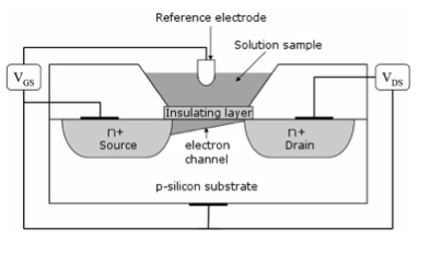
In this page you can learn various important field effect transistor questions answerssloved questions on field effect transistor and lots of important mcq on field effect transistor etc. A Field Effect Transistor FET is a three-terminal semiconductor device. On top of the substrate a thin layer of silicon dioxide SiO 2 the gate oxide is created via thermal oxidation.
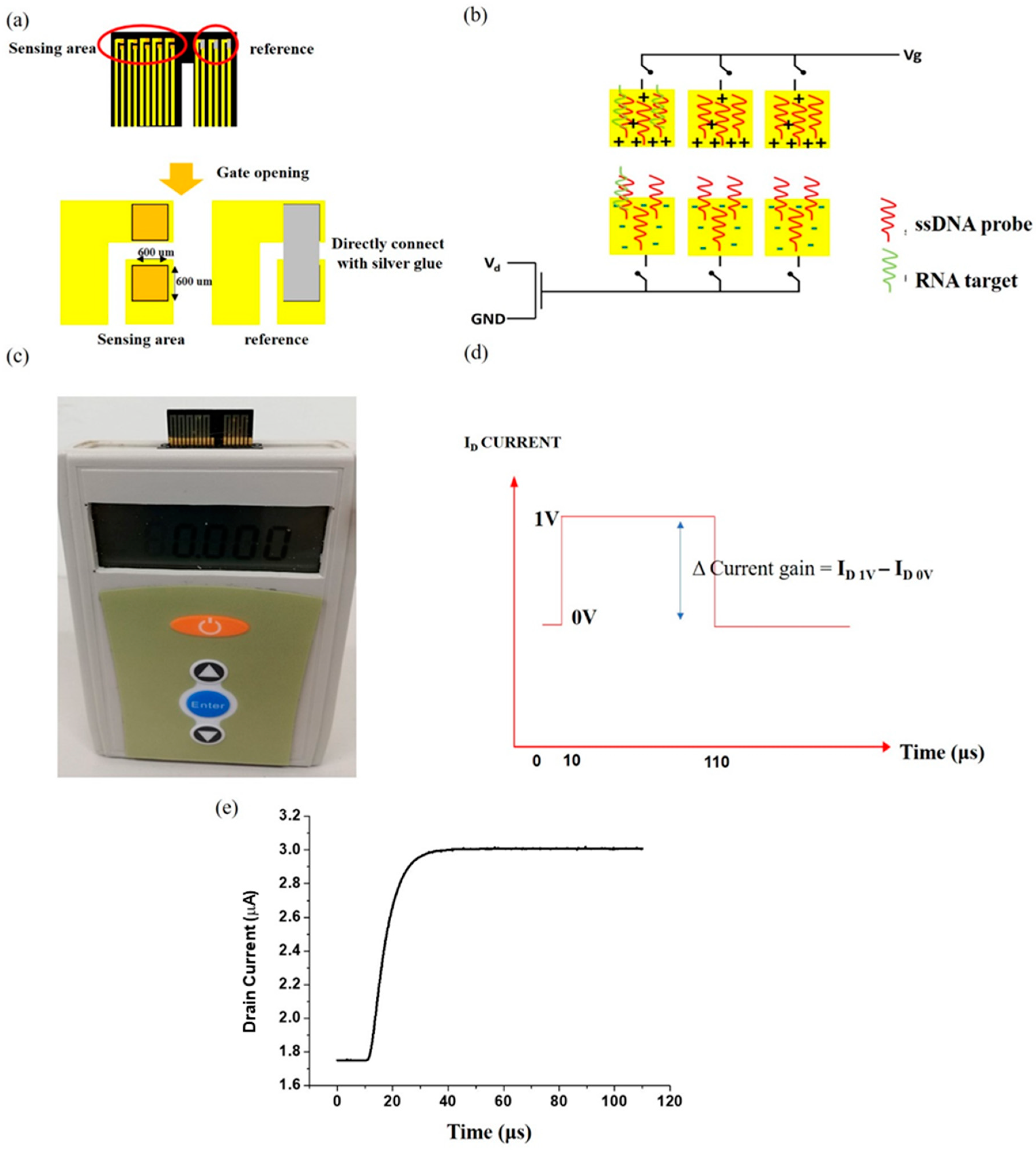
It is used for insulation of the later deposited gate and the substrate. The FET biosensor is gated by the biological molecules and it has a source and drain and can be connected example with nanowire. The field effect transistor FET mobility measurements also use the space charge injection into a normally undoped organic thin film similar to the SCLC method but a field is applied across a thin insulating layer gate in the direction perpendicular to the charge carrier transport which is determined by the source and.
Although there are lots of confusing names for field effect transistors FETs there are basically two main types. 7 positive with respect to the collector. If you are looking for a reviewer in Electronics Engineering this will definitely help.
The reverse biased PN junction types the JFET or Junction FET also. MC TCO 2 The n-type regions in an npn bipolar junction transistor are 7 points Week 10 Final Attempt 3Current Exam collector and base. Boylestad and Nashelsky Chapter 36 MC TCO 2 Which best describes a field-effect transistor.
7 A current-controlled device in which current at the base controls the collector voltage. However BJT is a current controlled device and JFET is controlled by input voltage. Junction Field Effect Transistors.
This is the Online Practice Quiz in Field Effect Transistor Devices Part 2 from the book Electronic Devices and Circuit Theory 10th Edition by Robert L. A cluster of field-effect transistor. By appearance JFET and bipolar transistors are very similar.
This is a simple explanation of what a field effect transistor is how it can be used and how its compared to the bipolar junction transistor. The metaloxidesemiconductor field-effect transistor MOSFET MOS-FET or MOS FET also known as the metaloxidesilicon transistor MOS transistor or MOS is a type of insulated-gate field-effect transistor that is fabricated by the controlled oxidation of a semiconductor typically siliconThe voltage of the gate terminal determines the electrical conductivity of the device. Its operation is based on a controlled input voltage.
This book provides an overview of Field Effect Transistors FETs by discussing the basic principles of FETs and exploring the latest technological developments in the field. It covers and connects a wide spectrum of topics related to semiconductor device physics physics of transistors and advanced transistor concepts. Collector base and emitter.
The field-effect transistor FET is a type of transistor that relies on an electric field to control the shape and hence the conductivity of a channel in a semiconductor material. TCO 2 Which best describes a field-effect transistor. Field effect transistor FET-based biosensors have two major components which are biological elements and electronic mediated FET sensing.
7 A current-controlled device in which current at the base controls the collector voltage. 233351 ii The field effect transistor mobility. It is very easy to understand and help you to improve your skill.
View TCO 2 A 1 A diode can deliver 1 A up to 75 C with a derating factdocx from AA 1 TCO 2 A 1 A diode can deliver 1 A up to 75 C with a derating factor of 85 mA C above that. Basis for a n-channel field-effect transistor is a p-doped boron silicon substrate. Most commonly two types of FETs are available.
FET sometimes is called unipolar transistor as it involves single carrier type operation. For various interview competitive examination and entrance test. TCO 2 In normal operation of an npn transistor the base must be Points.
Share your videos with friends family and the world.
![]()
Junction Field Effect Transistor Or Jfet Tutorial

Description Type Field Effect Transistor Brand Name International Rectifier Package Type Throught Hole Model Num Transistors Arduino 3d Printer Supplies
![]()
Junction Field Effect Transistor Or Jfet Tutorial
![]()
Understanding The Differences Between The N Channel And P Channel Field Effect Transistors Fets Technical Articles

Field Effect Transistors Fets As Transducers In Electrochemical Sensors Re Study Hix Hix
![]()
Understanding The Differences Between The N Channel And P Channel Field Effect Transistors Fets Technical Articles
Ion Selective Field Effect Transistor Lsi Epfl
![]()
Junction Field Effect Transistor Or Jfet Tutorial
![]()
Mosfet And Metal Oxide Semiconductor Tutorial
![]()
Junction Field Effect Transistor Or Jfet Tutorial
![]()
Understanding The Differences Between The N Channel And P Channel Field Effect Transistors Fets Technical Articles
![]()
7 Schematic Representation Of Field Effect Transistor Gas Sensor Where Download Scientific Diagram
![]()
Transconductance G M And Field Effect Mobility M Fe As A Download Scientific Diagram
![]()
Electrical Measurement Data Of Graphene Field Effect Transistors On Download Scientific Diagram

Electrolyte Gated Organic Field Effect Transistors For Quantitative Monitoring Of The Molecular Dynamics Of Crystallization At The Solid Liquid Interface Nano Letters
![]()
Understanding The Differences Between The N Channel And P Channel Field Effect Transistors Fets Technical Articles
![]()
Junction Field Effect Transistor Or Jfet Tutorial
![]()
Types Of Transistors
![]()
Junction Field Effect Transistor Or Jfet Tutorial


Comments
Post a Comment